STM32-Every: Compact STM32F411 Development Board
Hardware Project•JUL 2026
Overview & Design Objectives
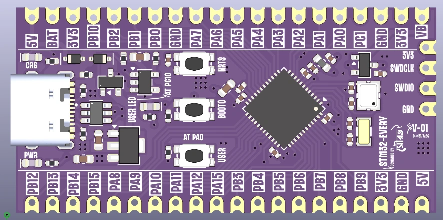
STM32-Every is a custom, feature-dense development board engineered in KiCad around the powerful STM32F411CEU6 ARM Cortex-M4 32-bit microcontroller (running at up to 100 MHz with 512 KB Flash, 128 KB SRAM, and hardware DSP/FPU).
While standard development boards like the classic Blue Pill or Black Pill lack integrated battery charging, ESD protection, and modern connectivity, STM32-Every was designed from the ground up to solve these constraints: incorporating a reversible USB Type-C interface, an onboard single-cell LiPo charger with automatic power-path selection, precision high-speed and real-time clock crystals, and dual castellated 20-pin headers for seamless breadboarding or SMT carrier module assembly.
While standard development boards like the classic Blue Pill or Black Pill lack integrated battery charging, ESD protection, and modern connectivity, STM32-Every was designed from the ground up to solve these constraints: incorporating a reversible USB Type-C interface, an onboard single-cell LiPo charger with automatic power-path selection, precision high-speed and real-time clock crystals, and dual castellated 20-pin headers for seamless breadboarding or SMT carrier module assembly.
Interactive 3D Autodesk CAD Model
Explore the full interactive 3D CAD model of the STM32-Every board below. You can orbit, zoom, pan, and examine all SMD components, castellated pin headers, buttons, and thermal pads directly in your browser:
Schematic Design & Subsystems
The schematic is divided into modular, high-reliability functional blocks:
• USB Type-C Interface: Reversible Type-C receptacle with dual 5.1 kΩ pull-down resistors (CC1/CC2) for standard 5V/3A negotiation and a dedicated DT1042-04S0-7 TVS array suppressing electrostatic discharge transients on USB D+/D- and VBUS lines.
• 1-Cell LiPo Charger & Power Path: Integrates an LTC4054ES5-4.2 constant-current/constant-voltage Li-Ion/LiPo battery management IC with onboard red
• Power Regulation & Analog Isolation: 3.3V power is delivered through a high-efficiency HT75xx-1 SOT-89 LDO with low-ESR ceramic decoupling capacitor banks. A ferrite bead (FB1) isolates digital VDD from analog VDDA to suppress high-frequency switching noise during precision ADC operations.
• Clock Generation & RTC: Features a 25 MHz High-Speed External (HSE) crystal for system PLL clocking, alongside a 32.768 kHz Low-Speed External (LSE) crystal connected with a BAT54C diode network for battery-backed Real-Time Clock operation.
• Control & Debugging: Includes dedicated tactile pushbuttons for Hardware Reset (
• USB Type-C Interface: Reversible Type-C receptacle with dual 5.1 kΩ pull-down resistors (CC1/CC2) for standard 5V/3A negotiation and a dedicated DT1042-04S0-7 TVS array suppressing electrostatic discharge transients on USB D+/D- and VBUS lines.
• 1-Cell LiPo Charger & Power Path: Integrates an LTC4054ES5-4.2 constant-current/constant-voltage Li-Ion/LiPo battery management IC with onboard red
CHRG status indicator. A low-Vf Schottky diode (1N5819WS) and P-channel power MOSFET (AO3401A) implement seamless automatic power switching between external USB and a 2mm JST battery connector.• Power Regulation & Analog Isolation: 3.3V power is delivered through a high-efficiency HT75xx-1 SOT-89 LDO with low-ESR ceramic decoupling capacitor banks. A ferrite bead (FB1) isolates digital VDD from analog VDDA to suppress high-frequency switching noise during precision ADC operations.
• Clock Generation & RTC: Features a 25 MHz High-Speed External (HSE) crystal for system PLL clocking, alongside a 32.768 kHz Low-Speed External (LSE) crystal connected with a BAT54C diode network for battery-backed Real-Time Clock operation.
• Control & Debugging: Includes dedicated tactile pushbuttons for Hardware Reset (
NRST), Bootloader mode (BOOT0), and User Input (PA0), plus a blue User LED (PC13), green Power LED, and a 4-pin ST-LINK SWD programming header (SWDIO, SWCLK, 3.3V, GND).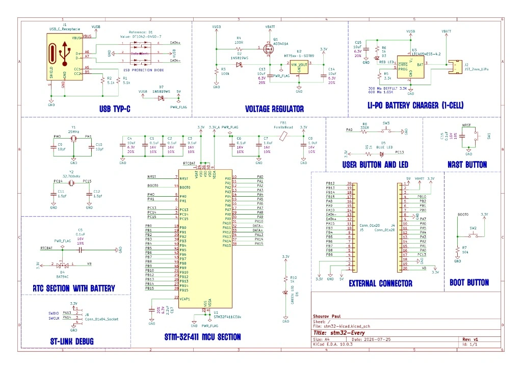
PCB Layout & Routing Strategy
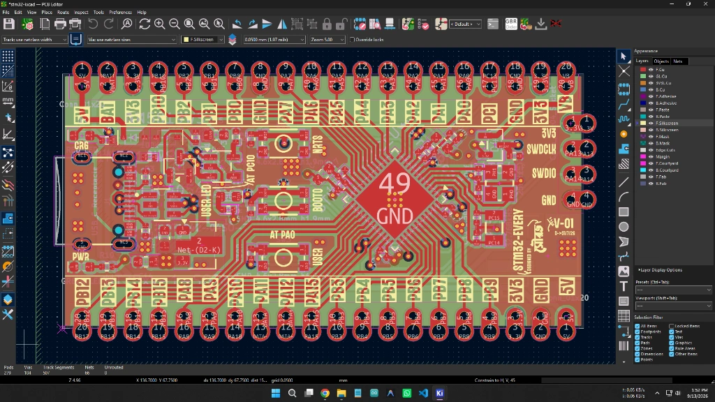
The PCB layout is designed for maximum signal integrity, thermal dissipation, and mechanical versatility:
• Thermal Relief & Ground Pour: Large copper ground planes on both top and bottom layers provide low impedance return paths, with a dense via matrix and 4.9 GND thermal polygon tying the central microcontroller ground pad directly to the ground planes.
• High-Speed Differential Routing: USB D+ and D- lines are routed with matched trace lengths, minimal via count, and continuous ground reference to guarantee clean eye diagrams for USB 2.0 Full Speed (12 Mbps) communication.
• Dual-Purpose Castellated Headers: Two 20-pin rows (0.1" / 2.54mm pitch) feature castellated edge pads, allowing the board to either be populated with standard male pin headers for breadboard prototyping or reflow-soldered flat onto a motherboard as an SMT compute module.
• Thermal Relief & Ground Pour: Large copper ground planes on both top and bottom layers provide low impedance return paths, with a dense via matrix and 4.9 GND thermal polygon tying the central microcontroller ground pad directly to the ground planes.
• High-Speed Differential Routing: USB D+ and D- lines are routed with matched trace lengths, minimal via count, and continuous ground reference to guarantee clean eye diagrams for USB 2.0 Full Speed (12 Mbps) communication.
• Dual-Purpose Castellated Headers: Two 20-pin rows (0.1" / 2.54mm pitch) feature castellated edge pads, allowing the board to either be populated with standard male pin headers for breadboard prototyping or reflow-soldered flat onto a motherboard as an SMT compute module.
KiCad 3D Assembly Inspection
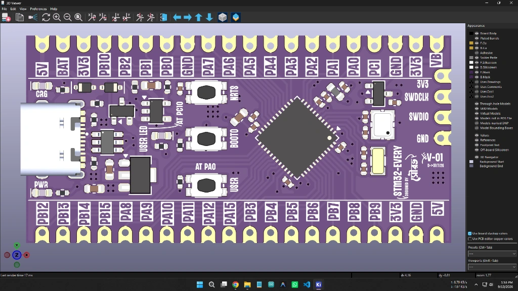
The fully rendered 3D board assembly highlighting component placement, solder mask clearance, and gold-plated castellated connector pads:
Firmware Core: System Clock & GPIO Configuration
main.c
1/*
2 * STM32-Every Hardware Test Firmware (STM32F411CEU6)
3 * Configures HSE (25MHz) to 100MHz System Clock and toggles User LED
4 */
5#include "stm32f4xx_hal.h"
6
7#define USER_LED_PIN    GPIO_PIN_13
8#define USER_LED_PORT   GPIOC
9#define USER_BTN_PIN    GPIO_PIN_0
10#define USER_BTN_PORT   GPIOA
11
12void SystemClock_Config(void) {
13  RCC_OscInitTypeDef RCC_OscInitStruct = {0};
14  RCC_ClkInitTypeDef RCC_ClkInitStruct = {0};
15
16  __HAL_RCC_PWR_CLK_ENABLE();
17  __HAL_PWR_VOLTAGESCALING_CONFIG(PWR_REGULATOR_VOLTAGE_SCALE1);
18
19  // Enable HSE (25 MHz) and configure PLL for 100 MHz SYSCLK
20  RCC_OscInitStruct.OscillatorType = RCC_OSCILLATORTYPE_HSE;
21  RCC_OscInitStruct.HSEState = RCC_HSE_ON;
22  RCC_OscInitStruct.PLL.PLLState = RCC_PLL_ON;
23  RCC_OscInitStruct.PLL.PLLSource = RCC_PLLSOURCE_HSE;
24  RCC_OscInitStruct.PLL.PLLM = 25;
25  RCC_OscInitStruct.PLL.PLLN = 200;
26  RCC_OscInitStruct.PLL.PLLP = RCC_PLLP_DIV2; // 100 MHz
27  RCC_OscInitStruct.PLL.PLLQ = 4;
28  HAL_RCC_OscConfig(&RCC_OscInitStruct);
29
30  // Set clock dividers for AHB, APB1, APB2
31  RCC_ClkInitStruct.ClockType = RCC_CLOCKTYPE_HCLK|RCC_CLOCKTYPE_SYSCLK
32                              |RCC_CLOCKTYPE_PCLK1|RCC_CLOCKTYPE_PCLK2;
33  RCC_ClkInitStruct.SYSCLKSource = RCC_SYSCLKSOURCE_PLLCLK;
34  RCC_ClkInitStruct.AHBCLKDivider = RCC_SYSCLK_DIV1;
35  RCC_ClkInitStruct.APB1CLKDivider = RCC_HCLK_DIV2;
36  RCC_ClkInitStruct.APB2CLKDivider = RCC_HCLK_DIV1;
37  HAL_RCC_ClockConfig(&RCC_ClkInitStruct, FLASH_LATENCY_3);
38}
39
40int main(void) {
41  HAL_Init();
42  SystemClock_Config();
43
44  __HAL_RCC_GPIOC_CLK_ENABLE();
45  GPIO_InitTypeDef GPIO_InitStruct = {0};
46  GPIO_InitStruct.Pin = USER_LED_PIN;
47  GPIO_InitStruct.Mode = GPIO_MODE_OUTPUT_PP;
48  GPIO_InitStruct.Pull = GPIO_NOPULL;
49  GPIO_InitStruct.Speed = GPIO_SPEED_FREQ_LOW;
50  HAL_GPIO_Init(USER_LED_PORT, &GPIO_InitStruct);
51
52  while (1) {
53    HAL_GPIO_TogglePin(USER_LED_PORT, USER_LED_PIN); // Blink PC13
54    HAL_Delay(500);
55  }
56}